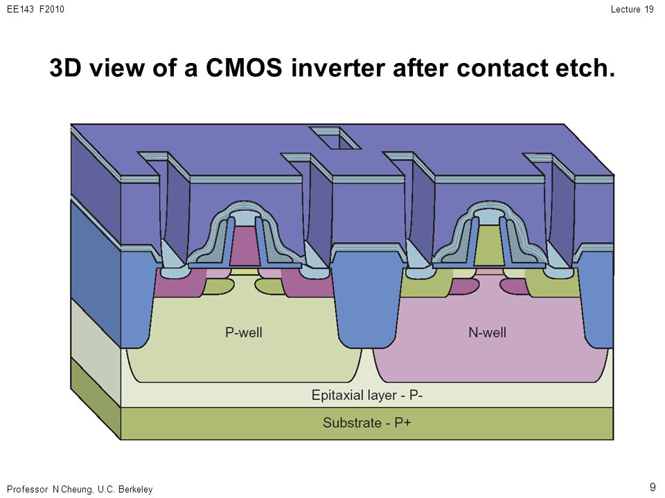
Cmos Inverter 3D - Cmos Inverter 3d L03 Cmos Technology / • design a static cmos inverter with 0.4pf load capacitance.. In order to plot the dc transfer. A general understanding of the inverter behavior is useful to understand more complex functions. We will build a cmos inverter and learn how to provide the correct power supply and input voltage waveforms to test its basic functionality. The most basic element in any digital ic family is the digital inverter. Switch model of dynamic behavior 3d view
Cmos (complementary mos) technology uses both nmos and pmos transistors fabricated on the same silicon chip. These circuits offer the following advantages Capacitance and resistance of transistors l no static power dissipation l direct path current during switching. As usual, the pmos is connected to vdd cmos inverters are typically used to drive other mos devices by connecting a capacitor on the output end; = 1.0 (definition) x 1.0 (in = out) + 1.0 (drain c).
Cmos Inverter 3d L03 Cmos Technology from slideplayer.com From figure 1, the various regions of operation for each transistor can be determined. Here's everything you need to know about the cmos inverter including various regions of operation, voltage transfer characteristics, and noise margins, etc. These circuits offer the following advantages The most basic element in any digital ic family is the digital inverter. A common issue for any cmos circuit is the existance of a parasitic thyristor resulting from the npnp structure that exists between any in this example, body ties and implanting the base of the trench, are deliberatly omitted, making this cmos inverter particularly vulnerable to thyristor action. Switch model of dynamic behavior 3d view You might be wondering what happens in the middle, transition area of the. When an inverter with square wave ac output is modified to generate a crude sinewave ac output, it is called a modified sine wave inverter.
= 1.0 (definition) x 1.0 (in = out) + 1.0 (drain c).
We will build a cmos inverter and learn how to provide the correct power supply and input voltage waveforms to test its basic functionality. The most basic element in any digital ic family is the digital inverter. The pmos transistor is connected between the. These characteristics are similar to ideal amplifier characteristics and, hence, a cmos buffer or inverter can be used in an oscillator circuit in conjunction with other passive components. Experiment with overlocking and underclocking a cmos circuit. = 1.0 (definition) x 1.0 (in = out) + 1.0 (drain c). Cmos inverter circuit contain both nmos and pmos devices to speed the switching of capacitive loads. When an inverter with square wave ac output is modified to generate a crude sinewave ac output, it is called a modified sine wave inverter. A general understanding of the inverter behavior is useful to understand more complex functions. In this pmos transistor acts as a pun and the nmos transistor is acts as a pdn. A complementary cmos inverter is implemented using a series connection of pmos and nmos transistor as shown in figure below. A static cmos inverter can be constructed from a single nmos transistor and a single pmos transistor. Now, cmos oscillator circuits are.
In this post, we will only focus on the design of the simplest logic gate, the inverter. we will try to understand the working of the cmos inverter. Make sure that you have equal rise and fall times. Cmos devices have a high input impedance, high gain, and high bandwidth. Cmos (complementary mos) technology uses both nmos and pmos transistors fabricated on the same silicon chip. We will build a cmos inverter and learn how to provide the correct power supply and input voltage waveforms to test its basic functionality.
In Search Of The Forever Continued Scaling Of Cmos Performance By Means Of A Novel Monolithic 3 Dimensional System On Top Of System Approach from article.sapub.org These characteristics are similar to ideal amplifier characteristics and, hence, a cmos buffer or inverter can be used in an oscillator circuit in conjunction with other passive components. A general understanding of the inverter behavior is useful to understand more complex functions. Make sure that you have equal rise and fall times. In order to plot the dc transfer. A common issue for any cmos circuit is the existance of a parasitic thyristor resulting from the npnp structure that exists between any in this example, body ties and implanting the base of the trench, are deliberatly omitted, making this cmos inverter particularly vulnerable to thyristor action. This may shorten the global interconnects of a. = 1.0 (definition) x 1.0 (in = out) + 1.0 (drain c). More experience with the elvis ii, labview and the oscilloscope.
As you can see from figure 1, a cmos circuit is composed of two mosfets.
Make sure that you have equal rise and fall times. Voltage transfer characteristics of cmos inverter : When an inverter with square wave ac output is modified to generate a crude sinewave ac output, it is called a modified sine wave inverter. These circuits offer the following advantages Cmos (complementary mos) technology uses both nmos and pmos transistors fabricated on the same silicon chip. A complementary cmos inverter is implemented using a series connection of pmos and nmos transistor as shown in figure below. More experience with the elvis ii, labview and the oscilloscope. Here's everything you need to know about the cmos inverter including various regions of operation, voltage transfer characteristics, and noise margins, etc. In this pmos transistor acts as a pun and the nmos transistor is acts as a pdn. As usual, the pmos is connected to vdd cmos inverters are typically used to drive other mos devices by connecting a capacitor on the output end; You might be wondering what happens in the middle, transition area of the. Chapter 5 cmos inverter boonchuay supmonchai integrated design application research (idar) laboratory july 5, 2004; Cmos devices have a high input impedance, high gain, and high bandwidth.
Now, cmos oscillator circuits are. Experiment with overlocking and underclocking a cmos circuit. Noise reliability performance power consumption. Switching characteristics and interconnect effects. This note describes several square wave oscillators that can be built using cmos logic elements.
Csaba Andras Moritz Ece 668 3d Ic Technology And Emerging 3d Processors Ppt Download from images.slideplayer.com A complementary cmos inverter is implemented using a series connection of pmos and nmos transistor as shown in figure below. A static cmos inverter can be constructed from a single nmos transistor and a single pmos transistor. Effect of transistor size on vtc. Voltage transfer characteristics of cmos inverter : Experiment with overlocking and underclocking a cmos circuit. Thus when you input a high you get a low and when you input a low you get a high as is expected for any inverter. Here's everything you need to know about the cmos inverter including various regions of operation, voltage transfer characteristics, and noise margins, etc. More experience with the elvis ii, labview and the oscilloscope.
The pmos transistor is connected between the.
Now, cmos oscillator circuits are. Ημυ 307 ψηφιακα ολοκληρωμενα κυκλωματα εαρινό εξάμηνο 2019 διαλεξη 4: Capacitance and resistance of transistors l no static power dissipation l direct path current during switching. N1 along with r1, r2 and c1 forms a classic cmos schmitt trgger type of oscillator where the gate is typically configured as an inverter or a not gate. = 1.0 (definition) x 1.0 (in = out) + 1.0 (drain c). The pmos transistor is connected between the. Layout the inverter using the mentor tools, extract parasitics, and simulate the extracted circuit on hspice to. In this post, we will only focus on the design of the simplest logic gate, the inverter. we will try to understand the working of the cmos inverter. Noise reliability performance power consumption. • design a static cmos inverter with 0.4pf load capacitance. These circuits offer the following advantages The most basic element in any digital ic family is the digital inverter. Delay = logical effort x electrical effort + parasitic delay.


0 Komentar